

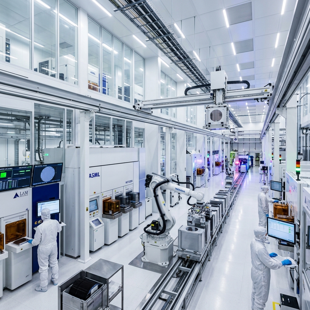
Tata-PSMC Mega Fab: Technical Specifications
The semiconductor fab in Dholera’s semiconductor corridor is designed to meet world-class manufacturing standards:
- Total Project Cost: ₹91,000 Crore (USD 11 Billion), supported by central and state capital subsidies.
- Technology Partner: Powerchip Semiconductor Manufacturing Corporation (PSMC), Taiwan.
- Wafer Capacity: 50,000 wafer starts per month (WSPM) at full scale.
- Silicon Wafer Size: 300mm (the industry standard for high-yield commercial chip production).
- Node Sizes: High-yield nodes at 28nm, 50nm, and 55nm, addressing the global demand for automotive power management, display drivers, microcontrollers, and computing chips.
Dholera Mega Fab Construction Milestones (2026)
The project has advanced through key engineering and structural phases:
1. Cleanroom Integrity and Safety
The structural shell of the main cleanroom (designed to Class 1 standards, maintaining less than 1 dust particle per cubic foot of air) has been completed. Specialized vibration-isolated flooring is in place to support high-precision lithography.
2. Equipment Installation
Installation of advanced lithography equipment from ASML (Netherlands) is currently underway. Chemical delivery lines and gas distribution grids are being routed to cleanroom terminals.
3. Dedicated Utility Corridors
Power supply is secured via a dedicated sub-station connected to Torrent Power’s smart grid, providing uninterrupted, dual-feed electricity. Water requirements are served by the DICDL high-purity recycled industrial water line.
Downstream Supply Chain Impact on Dholera Real Estate
The Tata Fab is attracting a cluster of secondary suppliers and chemical manufacturers to Dholera SIR:
- Fujifilm India’s chemical plant is establishing a supply base to deliver ultra-pure cleaning and etching chemicals directly to the fab.
- NextGen Semiconductors is setting up an ₹8,800 Crore sub-micron packaging and assembly plant in the adjacent corridor.
- This industrial concentration is driving massive demand for commercial plots, warehousing space, and residential housing for engineering teams, causing local land values to appreciate.
Frequently Asked Questions
1. When will commercial chip production begin at the Dholera Tata Fab?
Pilot wafer testing and initial calibration yields are scheduled for December 2026. Commercial mass production and distribution to clients are expected to commence in the second quarter of 2027.
2. How many jobs will the semiconductor hub create in Dholera?
The Tata mega-fab alone is estimated to create over 20,000 direct and indirect high-skilled jobs, which is fueling high demand for residential rental properties and co-living plots in TP1 and TP2.
Disclaimer: This article is published by the editorial team at Dholera Acres for informational purposes only. It does not constitute formal financial, legal, or investment advice. While every effort has been made to verify the semiconductor fab timeline, investment details, and infrastructure schedules with official DSIRDA publications, land investments are subject to market risks. Readers are strongly advised to perform independent legal due diligence and consult certified property advisors before making any transaction in Dholera SIR.
Download Dholera SIR 2026 Investor’s Kit
Get instant access to the official planning documents: Dholera Investment Handbook (PDF), 2026 Land Price List, TP Zone & Village Map, and the NRI Buying Guide.


Join The Discussion